Where the human body’s senses reach their limits, researchers develop tools to surpass them.
The eye draws conclusions about a material’s color and shape with a glance. The fingers determine a material’s temperature, malleability and texture with a touch. But the human body confirms few other qualities with certainty.
Instead of relying on human perception, researchers use sensors and imaging devices to perform spectroscopy, which measures the interactions between and matter to reveal a trove of information about a material.
Different molecules absorb and scatter mid-infrared light in distinct ways, similar to fingerprints. Light absorption analysis is used in a wide range of applications, from identifying chemicals in the air to diagnosing diseases and exploring planets. However, current detectors that work well in this range often require expensive cooling procedures or don’t perform well at room temperature.
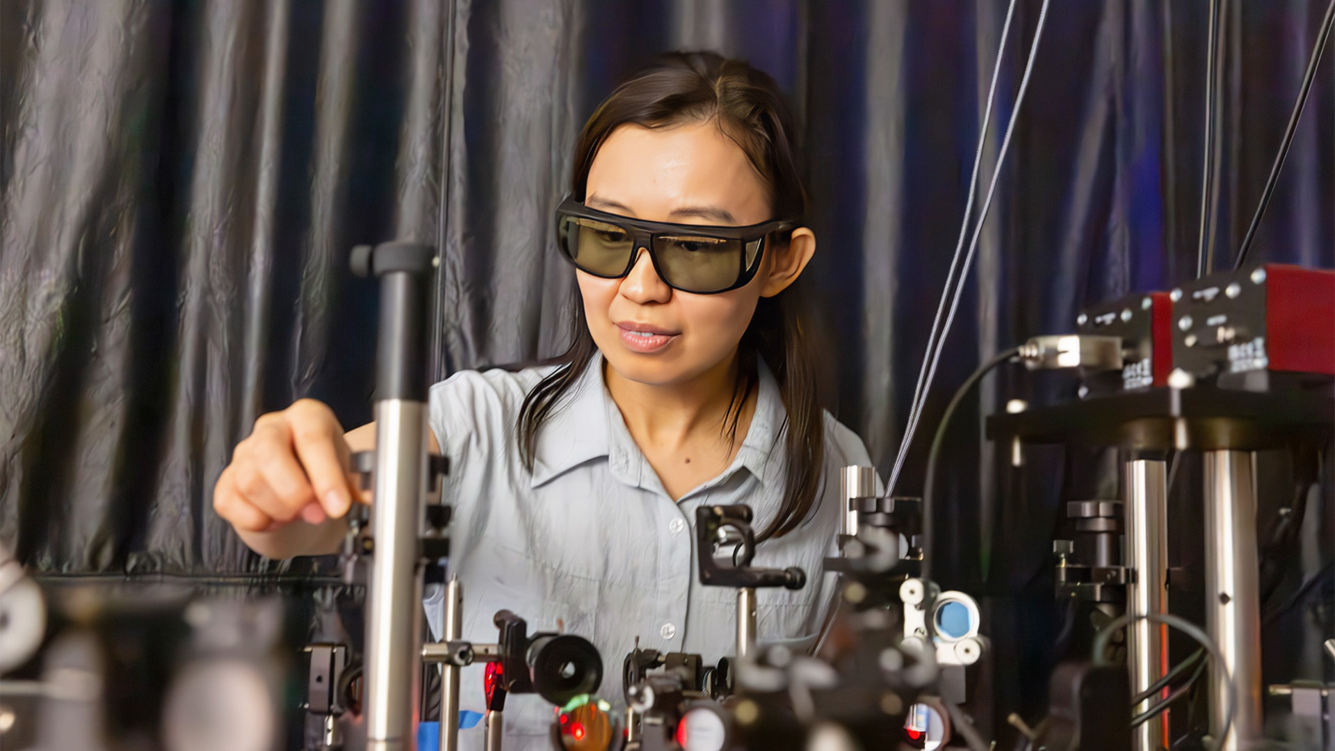
Yu Yao, an associate professor of electrical engineering in the School of Electrical, Computer and Energy Engineering, part of the Ira A. Fulton Schools of Engineering at Arizona State University, is developing more efficient, effective and compact sensors to bring advanced mid-infrared light sensing technology into new spaces.
“Any industry where someone needs to confirm a substance’s presence, or lack thereof, can benefit from advanced mid-infrared light sensing technology,” Yao says, “like using thermal imaging for security applications, gas analysis in environmental monitoring and classification in autonomous vehicles. Making the process affordable and scalable for manufacturing opens countless opportunities.”
Powering a sensitive sensor
In a recent Wiley publication, Yao outlines methods that diverge from conventional methods because they do not rely on traditional materials. Detecting infrared light requires semiconductors with much smaller dimensions than commonly used silicon-based photodetectors, which have greater costs and performance limits.
Zengyu Cen, an electrical engineering doctoral student in Yao’s lab, says their improvements tackle a critical pain point for the field.
“If you look at detectors for the infrared wavelength range, you’re going to find much more expensive detectors or imaging sensors with much worse performance compared with their visible counterparts,” Cen says. “It’s been a fundamental challenge for infrared and thermal imaging.”

To overcome these limitations, Yao’s team collaborated with Linbo Shao, an electrical engineering assistant professor at Virginia Tech, to redesign the device’s internal structure.
Their work yielded a system that uses a tiny vibrating structure made of mechanical parts that, when activated, slightly heats the material to manipulate its vibrational frequency.
The system then measures this change to precisely detect the light based on its absorption by nearby metasurfaces, which are patterned antenna-like structures designed to absorb specific wavelengths of light.
“The design and demonstration of such a mid-infrared detector involves microwave electronics, mechanics, acoustics and optics,” Shao says. “This is truly multi-disciplinary teamwork that requires researchers with different backgrounds working together to make a breakthrough.”
Yao says that historically, users have had to balance trade-offs between sensitivity, noise reduction and speed.
“This method improves the procedure’s sensitivity, response time and scalability while allowing opportunities to detect desired light wavelengths by customizing metasurfaces,” Yao says.
A scatter of applications
This research offers a powerful, precise and compact mid-infrared light sensor to advance the analysis that fuels how people interact with the world using light.
While light absorption analysis is already being used for diagnosing illnesses, monitoring vitals, space exploration, sterilizing equipment, assessing environmental pollutants and ensuring food safety, Yao is keen to see the method reach its full potential.
The Yao lab is actively collaborating with other researchers to explore the benefits of integrating light absorption analysis into various fields. It also opens the door to creating small, versatile sensor arrays for detecting multiple spectral regions of light on a single chip — a big step forward for miniaturized sensing technology.
“We can make many of these microscale detectors with standard semiconductor manufacturing processes, which is essential to eventually make affordable infrared detectors, chip-integrated infrared spectrometers and thermal imaging sensors based on our technology,” Yao says.
In the future, she aspires to see the sensors integrated into portable devices to help doctors during surgical operations, workers in factories to monitor industrial processes and safety conditions, autonomous vehicles to avoid crashing into pedestrians and animals in the dark or even everyday people to confirm the quality of their food, environment and health.


